


Recent advancements in machine learning have introduced innovative tools that enhance materials science, particularly in the semiconductor manufacturing industry. As challenges in this field become increasingly complex, AI-driven software is emerging to facilitate literature searches, simulations, and practical experiments, crucial for accelerating materials discovery and process optimization.
Key Features
The landscape of materials science problems is rapidly evolving, with an emphasis on identifying materials that can improve semiconductor manufacturing processes. Key issues include determining which metals exhibit the lowest resistance at nanowire dimensions and understanding the performance of various photoresists under extreme ultraviolet (EUV) light. The ongoing complexity in manufacturing has led to a significant increase in the number of materials involved, including previously rare elements like ruthenium and numerous auxiliary compounds that support the materials on the wafer.
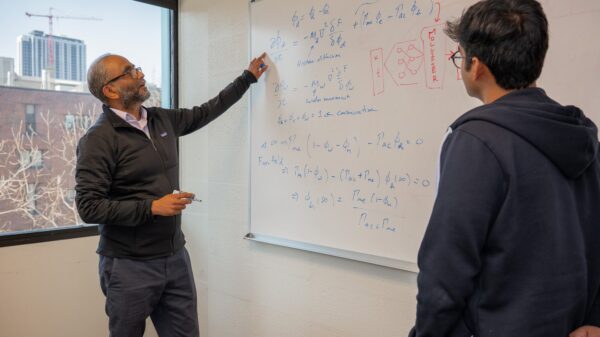
Machine learning tools are foundational in this area. They allow engineers to analyze extensive datasets that characterize material properties, some of which are derived from density functional theory (DFT) simulations. One notable breakthrough is the development of machine learning interpolated potentials (MLIPs), enabling the interpolation of potential fields between DFT simulations of reference systems, enhancing the understanding of defect-driven distortions in materials.
How the Tool Works
Materials discovery operates like a funnel, starting with a broad range of candidate materials and narrowing down to viable solutions. Engineers must formulate precise problem descriptions to optimize the search for materials, such as defining what constitutes a “better” interlayer dielectric. Existing data from literature and simulations combined with experimental studies create a robust framework for this exploration.
The integration of large language models (LLMs) plays a crucial role in analyzing accumulated materials knowledge stored in human-readable formats, such as technical journals. However, these models require retraining on specialized databases to yield the specific quantitative insights needed for materials discovery. This process allows researchers to identify promising materials that may not have been previously analyzed.
Furthermore, generative models are designed to create entirely new materials based on a defined set of desirable properties. They utilize training datasets of known materials to synthesize new candidates, which can then be evaluated through simulations, effectively bridging the gap between theoretical models and practical applications.
Use Cases and Who It’s For
The primary beneficiaries of these AI-driven tools are research and engineering teams in semiconductor manufacturing and materials science. The ability to rapidly screen and evaluate hundreds to thousands of candidate materials accelerates the development of next-generation devices with improved performance characteristics. Such AI tools enable engineers to focus on a narrower range of candidates that show promise based on both simulation results and experimental data.
As the semiconductor industry seeks to enhance efficiency and performance, the integration of AI allows engineers to make informed decisions that align with the rapidly changing landscape of materials science. The effectiveness of these tools lies in their ability to analyze large datasets quickly, reducing the time from material concept to practical application.
Limitations or Risks
While AI tools significantly enhance the materials discovery process, they are not without limitations. For instance, DFT methods remain computationally intensive and are best suited for ideal crystals, struggling with disordered systems and defects that are common in real materials. Additionally, as materials progress from initial screening to process integration, experimental validation becomes increasingly essential. AI tools cannot replace experimentalists but can guide focused examinations of a tailored set of candidates.
Overall, the synergy of advanced AI techniques and traditional materials science methodologies is transforming the landscape of semiconductor manufacturing. These tools not only streamline the discovery process but also enable researchers and engineers to tackle previously insurmountable challenges in material integration and performance optimization.
See also Google Unveils Gemini 3, Achieving Breakthroughs in Multimodal Reasoning and Interactivity
 Patients Embrace AI in Healthcare with Doctors Retaining Oversight, Study Finds
 Check Point Partners with Microsoft to Embed AI Security in Copilot Studio
 Meta Develops AI Briefing Tool ‘Project Luna’ for Personalized Facebook Summaries
 Microsoft AI CEO Mustafa Suleyman Criticizes Public’s AI Skepticism Amid New Innovations