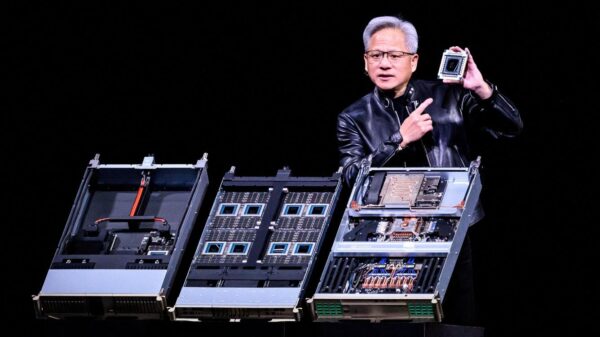
The race for AI computing power is intensifying, prompting urgent discussions about the sustainability of chip technology. As the demand for advanced computing capabilities surges, concerns are mounting over the overheating of next-generation processors. Notably, NVIDIA’s H100 chip has a peak power consumption exceeding 700W, with projections indicating that the forthcoming Rubin processor could reach as high as 1800W. By 2029, this figure is expected to soar to 6000W, raising alarms about the limitations of current packaging technologies.
Traditional silicon interposers, essential for connecting chips, are struggling to manage heat dissipation effectively and are susceptible to cracking. Meanwhile, the ‘power wall’ associated with CoWoS packaging is emerging as a critical bottleneck in the pursuit of greater performance. Industry experts argue that a shift toward advanced packaging solutions, particularly those incorporating Silicon Carbide (SiC), is essential to overcoming these challenges.
In a concerted effort to address these issues, Taiwan Semiconductor has issued a broad call to action to enhance SiC interposer technologies. Companies are already taking steps to adapt, with NVIDIA planning to adopt 12-inch SiC substrates by 2027. This shift has begun to manifest in the A-share market, where advanced packaging stocks have seen significant growth—an over 14% increase since the year’s start. Jiangsu Changjiang Electronics Technology, for example, experienced a trading volume exceeding 5 billion yuan, highlighting the market’s robust response to the intersection of AI demand, SiC breakthroughs, and domestic supply replacements.
The increasing requirements for AI model training and data center operations are prompting a paradigm shift in the semiconductor industry. By 2025, it’s anticipated that China’s intelligent computing capabilities will reach 1037.3 EFLOPS, with an expected 40% growth by 2026. Traditional packaging methods cannot meet this surging demand, as power consumption rises disproportionately to performance—every doubling of chip performance comes with a tripling of power consumption. The thermal conductivity of existing silicon interposers, just 148 W/m·K, falls drastically short of what is needed for ultra-high power chips.
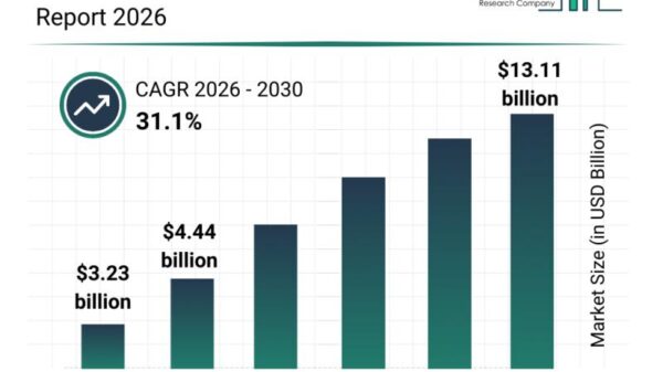
Advanced packaging technologies like 2.5D and 3D stacking, along with hybrid bonding techniques, are now viewed as vital solutions. These innovations can enhance chip interconnection density tenfold and significantly mitigate heat-related issues. According to projections by Yole, the global advanced packaging market is set to exceed $79 billion by 2030, with 2.5D and 3D packaging experiencing an annual growth rate of 37%. This marks a significant shift in the landscape, highlighting the industry’s need to adapt rapidly.
The continuous iteration of technology from 2.5D to SiC underscores the dynamic nature of advanced packaging. The shift from traditional silicon interposers to SiC represents not just a material change but a broader opportunity for process innovation. For instance, 3D packaging can achieve copper-to-copper direct connections via hybrid bonding technology, reducing signal delay by 30%. Major players like Taiwan Semiconductor and Intel are already implementing these technologies, with large-scale applications expected by 2026.
SiC’s superior thermal conductivity of 490 W/m·K, compared to silicon’s, offers a solution to existing constraints, enabling designs that optimize wiring density and enhance chip transmission speeds. By 2027, mass production of SiC interposers is anticipated, which could generate a substantial demand for 12-inch substrates, projected to exceed current global capacities. This expected shortfall presents both challenges and opportunities for companies positioned within the supply chain.
The rise of advanced packaging is reshaping the semiconductor industry, creating a ripple effect across equipment, materials, and outsourced semiconductor assembly and testing (OSAT). The OSAT sector is experiencing significant benefits, with companies like Changdian Technology and Tongfu Microelectronics making notable advancements in packaging solutions. Meanwhile, localizing the production of critical materials used in packaging—such as substrates, PSPI, and CMP polishing fluids—has become pivotal for reducing dependency on international suppliers.
Equipment manufacturers are also stepping up, with Chinese firms now breaking into previously foreign-dominated markets with innovations in hybrid bonding machines and CMP equipment. As the semiconductor packaging equipment market is expected to reach 28.27 billion yuan in 2024—up 18.9% year-on-year—the demand for these technologies will only increase as SiC interposers move to mass production.
Looking ahead, the advanced packaging industry is set on a transformative path, transitioning from a mere auxiliary element of semiconductor processes into a core driver of computing power. The combination of escalating AI demands, technological advancements in SiC, and a strong push for domestic substitutes is positioning this sector for explosive growth. As industry stakeholders monitor the mass production timeline for SiC interposers and advancements in technology, opportunities for investment will arise across various facets of the semiconductor supply chain.
See also Geekom Launches GeekBook X16 Pro: Affordable 16-Inch AI Laptop Starting at $1,149
 Japanese Researchers Unveil Ultrafast Laser Method to Control Chip Heat at Nanoscale
 AI Data Centers Face Engineer Shortage; U.S. Needs 400,000 Workers by 2033
 AI Tools Enhance Diagnosis Accuracy Amid U.S. Healthcare System’s Resource Crisis
 South Korea Downplays Impact of 25% US Tariff on AI Chips, Excludes Memory Products

