


Japanese researchers have developed a novel method for managing heat within electronic components that significantly alters traditional cooling approaches. Unlike current reliance on heat sinks, fans, or liquid cooling systems to dissipate heat after it accumulates, this innovative technique allows engineers to control the rate at which heat escapes from materials, specifically thin silicon and silica films. The findings were detailed in a recent study published by the Institute of Science Tokyo.
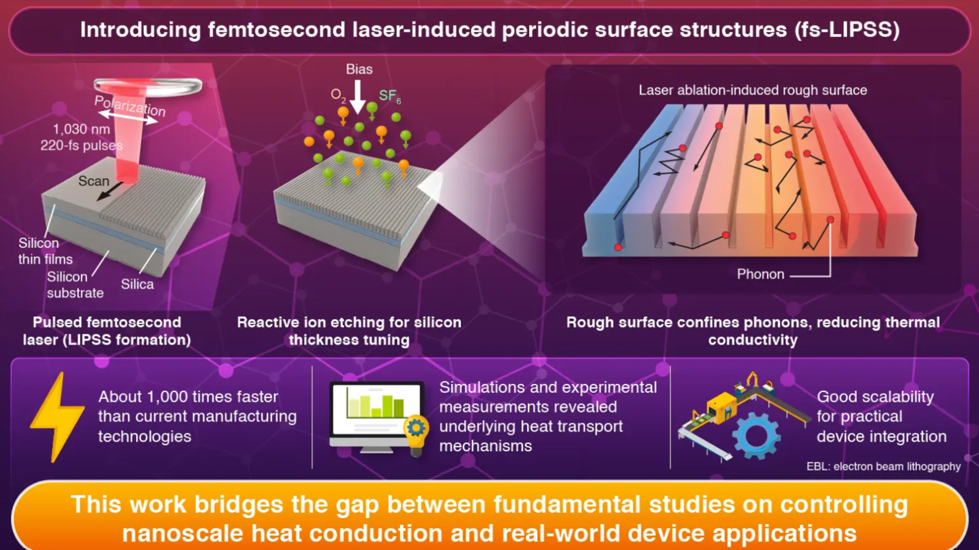
The method employs ultrafast laser pulses lasting just a femtosecond, enabling the precise ablation of material to create periodic surface structures. These grooves, formed with meticulous spacing and depth, closely correspond to the average travel distance of phonons—particles that are principal carriers of heat in these materials. By restricting phonon movement, researchers can predictably modify the thermal conductivity of the chips.
The newly developed features, termed femtosecond laser-induced periodic surface structures, exhibit a high degree of uniformity across larger areas. When combined with traditional dry etching techniques to fine-tune film thickness, these patterned surfaces demonstrate a significant reduction in thermal conductivity. This reduction was confirmed through thermoreflectance measurements and supported by numerical simulations, which indicated that the primary factor was limited phonon travel rather than changes in chemical composition or bulk material properties.
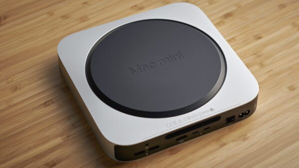
A key advantage of this method is its speed. The femtosecond laser-induced periodic surface structures (fs-LIPSS) process reportedly operates over 1000 times faster than conventional single-beam electron-beam lithography while maintaining nanoscale resolution. This rapid throughput is particularly beneficial for applications requiring extensive patterned areas, such as thermal layers in data center-class processors. The method is also maskless and resist-free, simplifying procedural complexity and aligning with existing CMOS manufacturing processes.
In addition, the researchers assert that the technique can be implemented on a wafer scale without introducing new components or lithographic steps, enhancing its compatibility with established semiconductor workflows. The mechanical robustness of the nanostructures produced is noteworthy as well, with preliminary reports suggesting strength levels up to 1000 times greater than those achieved through some traditional patterning techniques. However, specific details on direct mechanical benchmarking or comparative testing remain limited.
This promising approach could have wide-ranging implications for high-performance computing, quantum devices, and the thermal management challenges posed by densely packed GPU clusters that drive modern AI tools. Nevertheless, broader adoption hinges on ensuring reproducibility, long-term stability, and cost-effectiveness under industrial conditions, particularly at the scale required for data centers.
The ongoing evolution in heat management technologies highlights a critical area of research as electronic devices continue to increase in power and complexity. As this innovative laser-based fabrication method demonstrates potential advantages in speed and efficiency, it represents a significant step forward in addressing thermal challenges in contemporary computing environments.
See also AI Data Centers Face Engineer Shortage; U.S. Needs 400,000 Workers by 2033
 AI Tools Enhance Diagnosis Accuracy Amid U.S. Healthcare System’s Resource Crisis
 South Korea Downplays Impact of 25% US Tariff on AI Chips, Excludes Memory Products
 Taiwan Invests $250B in U.S. Tech to Boost AI Chip Production Amid Trade Deal
 Alphabet Commits $93 Billion to Quantum Computing, Targets Industry Leadership