


Artificial intelligence (AI) systems are rapidly becoming significant energy consumers, with a single request to ChatGPT requiring approximately ten times the power of a Google search. This soaring demand is projected to escalate, with estimates indicating that the popular chatbot could consume around 40 million kilowatt-hours (kWh) of electricity per day—enough energy to charge nearly eight million smartphones, equating to almost every phone in New York City.
As AI tools evolve to be more powerful and personalized, their energy requirements are expected to increase dramatically. According to the Lawrence Berkeley National Laboratory (LBNL), by 2028, over half of the electricity used by data centers could be driven by AI workloads. Such a scenario could see AI systems consuming as much electricity annually as all U.S. households combined. With data center power demands rising by roughly 15 percent each year, researchers are actively seeking methods to enhance the energy efficiency of AI.
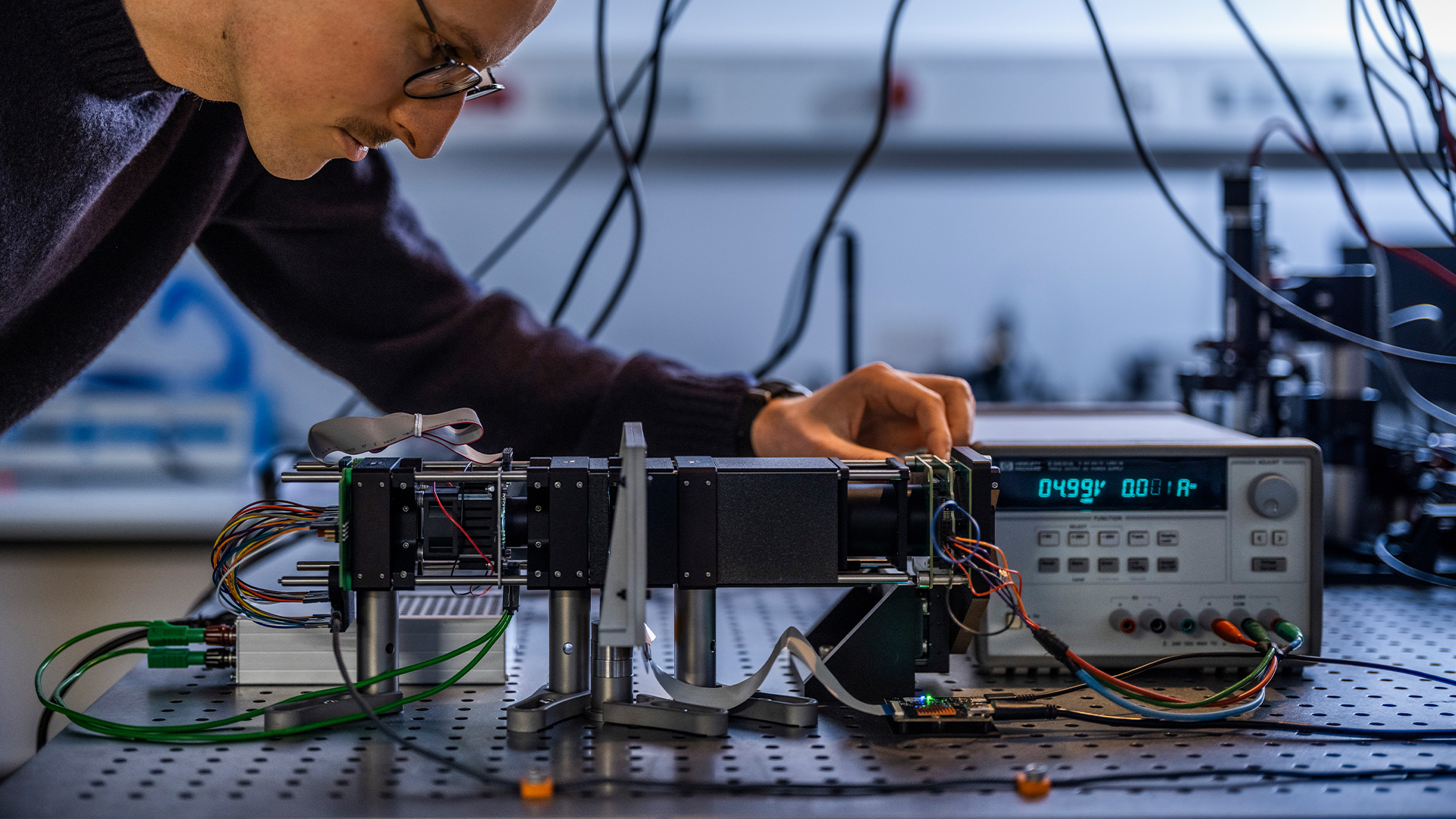
Scientists at Germany’s Technische Universität Braunschweig (TU Braunschweig) are exploring gallium nitride (GaN) as a potential alternative to silicon in semiconductor technologies. This material, known for its high electron mobility and thermal stability, is being investigated as part of the Bringing Light to Microelectronics (BRIGHT) project. By integrating tiny GaN microLEDs with silicon electronics, the team aims to develop a novel type of optical neuromorphic hardware that processes information using light instead of electricity.
GaN is a compound semiconductor consisting of gallium and nitrogen and belongs to the category of wide-bandgap (WBG) semiconductors. With a melting point around 2,912°F (1,600°C), GaN is suitable for high-power and high-frequency electronic devices, including LEDs and laser diodes. Historically, GaN was considered unsuitable for semiconductor applications due to its imperfect crystal structure, which contained more than one billion defects per square centimeter, compared to fewer than 100,000 for typical LED materials.
This perception shifted in the early 1990s when researchers Isamu Akasaki and Hiroshi Amano, alongside Shuji Nakamura, developed high-brightness blue LEDs using GaN, a breakthrough that earned them the 2014 Nobel Prize in Physics. Andreas Waag, PhD, managing director of the Institute of Semiconductor Technology at TU Braunschweig, noted that GaN’s evolution has made it central to modern electronics.
Neuromorphic computing, which emulates human brain processes, represents a potential path forward in reducing the energy requirements associated with traditional AI models. Current AI systems typically demand vast amounts of energy for training and operation; however, neuromorphic chips, inspired by the brain’s ability to function on approximately 20 watts, utilize sparse, event-driven processing that activates circuits only when necessary. Consequently, neuromorphic processors can perform complex AI tasks while consuming significantly less energy than conventional CPUs or GPUs.
Nevertheless, integrating traditional silicon electronics into neuromorphic systems complicates the physical wiring of connections between artificial neurons, limiting the scalability and efficiency of these systems. According to Waag, microLEDs could circumvent this challenge by allowing light signals to be detected by millions of sensors without the need for physical wiring. This approach is central to the BRIGHT initiative, which combines expertise from leading microelectronics groups.
In the BRIGHT project, Waag explained that GaN’s unique properties allow for the creation of minuscule LEDs that emit light efficiently. This capability could lead to optical systems with high information density that operate on light rather than electrical signals, facilitating massively parallel interconnectivity. The initiative, backed by €15 million (approximately $17.5 million) from the State of Lower Saxony and the Volkswagen Foundation, aims to combine GaN microLEDs with silicon-based integrated circuits.
This hybrid strategy seeks to merge high-density electronic processing with efficient optical signal transmission, potentially enabling faster and more energy-efficient AI hardware. Waag emphasized that if millions of microLEDs could be driven in parallel by silicon chips, the resulting high-bandwidth data streams could transform AI applications. The project has even led to the establishment of a startup, Synara Technologies, which is exploring commercialization opportunities.
As AI continues to expand, the energy demands of large computing centers could become unsustainable, with estimates projecting that by 2035, AI could account for 30 to 40 percent of global electricity use. Waag highlighted the urgency of prioritizing energy efficiency in future AI infrastructure. He further noted that while silicon CMOS technology is predominantly controlled by Asia and the United States, Europe retains a strong position in GaN technology, presenting an opportunity to bolster its technological standing.
Looking ahead, researchers are optimistic about the prospects of integrating GaN into modern processors. Waag believes that while current processors are entirely silicon-based, the next decade could see gallium nitride incorporated into more advanced chips, enhancing their capabilities and energy efficiency. As the BRIGHT project progresses, it could pave the way for sustainable, high-performance AI systems capable of meeting the growing energy challenges posed by the sector.
See also AI Infrastructure Stocks Everus, Sterling, and Flowserve Drop 9% – Time to Buy?
 Affordable Android Smartwatches That Offer Great Value and Features
 Russia”s AIDOL Robot Stumbles During Debut in Moscow
 AI Technology Revolutionizes Meat Processing at Cargill Slaughterhouse